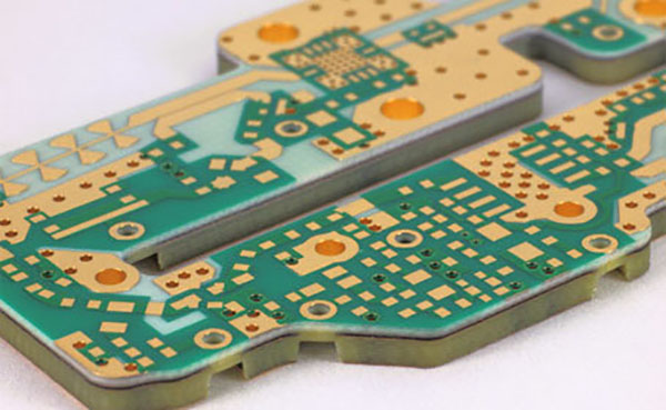
Multi-layer Mixed Dielectric PCB

Multi-layer Mixed Dielectric PCB
Consisting of multiple laminates and differing dielectric constants, this multilayer (displayed above) is a mixed-dielectric printed circuit board which was manufactured by Standard Printed Circuit, Inc. for the Aerospace Industry. Beginning with Inventory, all the correct materials were pulled and checked against customer requirements and specifications.
Initially, all innerlayers were drilled, imaged, and etched. The innerlayers then proceeded to Lamination where they were pressed into panels using low Dk bonding films. After lamination and cool-down, the panels moved to drilling where all primary holes were drilled. To prepare the hole walls for Direct Metallization, the panels were processed through Plasma and Sodium etching.
After DMS, the outer layers of the panels were imaged, copper plated, solder plated, and etched. Trace widths had to be controlled to +/- .0005″ to provide the end product with proper electrical characteristics. A Liquid Photoimageable (LPI) soldermask was applied, followed by a ENIG (Electroless Nickel Immersion Gold) final finish. Using a number of product evaluation techniques, including flying probe testing, we ensured that this PCB met with all client product requirements. By the end of this project, our company manufactured 75 multilayer, mixed- dielectric printed circuit boards for this aerospace customer, vacuum packaging and shipping all completed items to their facility in Northeastern US.
Multi-layer Mixed Dielectric PCB Highlights
Product Description
This Multi-Layer Mixed Dielectric PCB is used within an Aerospace application and contains different laminates and structures.
Capabilities Applied/Processes
Shearing
Inner layer Fabrication (Image, Etch, and Oxide)
Multilayer Lamination
CNC Drilling
Deburring
Prep Hole Wall
- Plasma Etching
- Sodium Etching
Direct Metallization
Photolithography
Plating
Etching
LPI Soldermask / Silkscreen
ENIG Plate
- Electroless Nickel- Immersion Gold.
Final Fabrication
Packaging
Equipment Used
Alternative Oxide Line
CNC Driller
CNC Router
ENIG Line
Etcher
Exposure, Developer
Flying Probe Electrical Test
Plasma Etch / Sodium Etch
Vacuum Lamination Press.
Overall Part Dimensions
Layers: 6
Length: 3"
Width: 1.5"
Tightest Tolerances
±.0005" on Etched Features
Material Used
Ceramic filled PTFE, Multi-functional FR4
Material Finish
Electroless Nickel - Immersion Gold
Estimated Part Weight
20 Grams
In process testing performed
Cross Section Analysis
Full Electrical Test
Line Width Verification
Industry for Use
Defense/Aerospace
Quantity Manufactured
75
Delivery Location
Northeast US
Standards Met
IPC-6018 Microwave End Product Board Inspection and Test
IPC-A-600 Acceptability of Printed Boards
Product Name
Multi-Layer Mixed Dielectric PCB (Printed Circuit Board)