MULTI-LAYER PCBS

MULTI-LAYER PCBS
What’s the definition of a multilayer PCB?
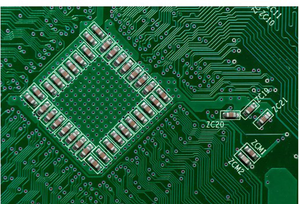
Many printed circuit boards have one or two conductive layers, being built on either a double-sided or a single-sided substrate. A multi-layer PCB is designed and manufactured using several layers of base material. Generally speaking, any board featuring at least three conductive layers is included in this category.
Multilayer PCBs are constructed using a ‘sandwich’ model, featuring numerous double-sided conductive layers separated by a corresponding number of insulating material sheets. These must all be bonded and laminated together under high pressures and temperatures, such that no air gaps remain and the final PCB assembly is sufficiently robust.
Are multilayer PCBs better than double-sided?
The answer here depends on the finished board’s intended application. While multi-layer designs are more expensive to produce, there are numerous scenarios in which they’re beneficial or essential. This is often because they allow for more complex circuits in a smaller footprint. Key advantages of multi-layer PCBs may include:
- Improved durability – more layers stacked together makes for a more robust physical design
- Overall quality – they’re inherently more complex to design and , meaning the production process is often more meticulous
- Better for more complex or high-power circuit designs – speed and capacity requirements for some performance devices may demand a multilayered
- Space-saving – stacking conductive layers allows for reduced footprint, with larger circuits fitting on a smaller and more lightweight board
- Single connection point – multiple separate PCBs would each need to be powered individually; a muti-layer design usually has just one such input
How are they manufactured and assembled?
You can see a more comprehensive breakdown of exactly how a standard PCB is constructed in our guide to the PCB manufacturing process. As well as a detailed workflow infographic, this page includes a series of our own in-house videos showing precisely how each phase is carried out.
Production of a multi-layer PCB follows much the same core process. However, the manufacturing stage will include additional steps for physically assembling and laminating the more complex substrate that supports the circuitry and components.
What are multi-layer PCBs used for?
ABL Circuits are established industry experts in the design and manufacture of multi-layer PCBs. These typically offer increased functionality for computers and laptops, mobile phones and tablets, medical equipment, GPS trackers, and many other more complex circuits and devices.