HDI PCBS

HDI PCBS
What are HDI PCBs
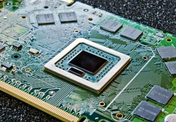
HDI PCBs, known as High Density Interconnect PCBs, are one of the fastest-growing technologies available in the circuit board world. HDIs have higher circuitry density compared to more traditional circuit boards, such as single sided or double sided PCBs, and their design allows them to have smaller vias, smaller capture pads alongside higher connection pad densities.
HDI PCB benefits
This HDI technology allows designers and manufacturers to place more components on both sides of the PCB, if needed for your products. HDI boards also contain blind and buried vias, alongside micro vias which have a smaller diameter meaning designers are also able to place smaller components closer together on the board, resulting in quicker transmission of signals across and less signal loss or crossing delays.
The finer structures of a HDI PCB means they are extremely compact in size and have fewer layers compared to multi-layer PCBs, allowing for greater packaging density. Whilst they may be smaller in size, the HDI micorvia technology used to produce these boards means an 8 layer through-hold PCB can be reduced to a 4 layer HDI PCB whilst still having the same, or improved functions of a standard 8 layer PCB. Subsequently, what an HDI PCB lacks for in size, it makes up for in quality.
DI PCB manufacturing
If you thought that the manufacturing of HDI PCBs would require special equipment or additional time, you would be right, as several processes and particular equipment are needed to assemble these high-quality boards. Laser drill technology is needed to drill the small micovias, which allow for additional technology on the board. The lamination process of HDI PCBs is also more complex, due to the fact they are multi-layer boards constructed with densely routed layers.
Applications of HDI PCBs
Whilst the manufacturing process may be slightly more complex, the product you are left with can be used in a range of products across various industries. HDI PCBs are used in advanced technology systems such as smartphones and games consoles. They are also making a huge impact on the medical industries as their small size means they can fit in devices such as imaging equipment for miniature sized cameras, which help doctors in their patient diagnosis, without impacting the picture quality.
HDI PCBs have become popular due to their small size, high quality and versatility. With HDI design, ABL Circuits can help design and manufacture the perfect board for your next product. Get in touch for the team for more information on these innovative boards.