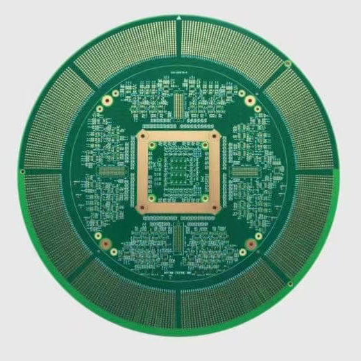
HDI PCB – High Density Interconnect PCB

HDI PCB – High Density Interconnect PCB
HDI PCB (High Density Interconnects PCB) are used to meet the market demand for complex designs in smaller form factors across the majority of market segments, (Wireless, Telecom, Military, Medical, Semiconductor, and Instrumentation).
What is HDI PCB ?
- The HDI PCB is the short form of High-Density Interconnect Printed Circuit Boards.It has been constructed by using HDI technology for a compact and reliable PCB design.
- It characterizes the high-density attributes including laser micro vias, fine lines as well as the high performing materials.
- The traditional PCBs are covered with copper throughout the inner and outer layers ,Where as the HDI PCBs are incorporated with multi-layers of copper filled with stacked micro-vias.
- It creates a structure enabling complex interconnections to provide necessary routing solutions.The high tech applications are utilizing the advantages of the functional strategy of the HDI PCB to construct the large pin-count chips.
Structural definition of HDI PCB
- The higher circuitry density is the main reason behind its naming.
- The HDI PCB is designed with typically smaller vias and capture pads, finer lines and specs, and high connectivity of pad density.
- The combination of the fine track and gap features with the laser-drilled blind allows the interconnection with one PCB layer to the other using the smallest pad diameter.
- The HDI boards include a blind and buried vias in size of 0.004 diameters for the micro-vias.It creates greater flexibility in the architecture of the HDI PCB by the utilization of increased efficiency.
- The HDI PCB consists of 1 or more than 1 “build-up” of high-density interconnection layers staggered or stacked micro vias on different layers.
- All the layers of this PCB enable the conductors on any layer of the PCB to be interconnected freely with copper filled stacked micro-vias structures.It creates a reliable interconnection solution for highly complex large-pin count devices such as CPU and GPU chips to improve the portable devices.
- By utilizing the HDI technology, the designers are now able to place smaller components closely for faster transmission of signals. This helps in a significant reduction in loss of signals and crossing delays.
Using this HDI PCB will enhance the functioning improving:
- Dense trace routing
- Extended power stabilization
- Reduced interference effects into the inductance and capacitance
- Improved signaling integrity for the high-speed applications
- Decreases frequent relocating the components
Increases the space for the other components
Andwin maintains years of experience with HDI products and was a pioneer of second generation microvias. now offer an entire family of microvia technology solutions for your next generation products.
Feature of HDI PCB
The HDI is an efficient and durable solution for creating high-functioning applications in a lighter and smaller format. Along with all the improved functionality in smaller consumer products, denser BGA, and QFP packages it lowers the heat transfer induced by stress. The following features reflect the working process of HDI PCB in the applications:
- The HDI PCB can get populated from both sides of the board and incorporate the components onto smaller boards.
- It decreases the power consumption and leads to having longer stand-by facility into the handheld and other battery-powered devices.
- It comes in a well-built and rugged format to provide strength and limited perforations.
- The reduced thermal degradation extends the endurance of the device.
- The device can have higher density transmission and computational features using a smaller space.
- The HDI PCB uses and accommodates with sustainable and dense BGA and QFP packages in PCB technology design to create smaller devices based on the user’s demand. It can be smartphones, aerospace equipment, medical applications, or military devices.
It enhances reliability in transmission whereas the PCB design gets into the point of mass production.
Benefits of HDI PCB
By the evolution of high-density PCB technology, the engineers are having enough freedom and flexibility in designing the applications according to consumer demands. They get space to place the components on both sides of the raw PCB. It consists of the following key benefits:
- Concentrated Transfer of Heat:The transfer of heat is reduced due to the close placement of the components. The thermal expansion in HDI PCB also endures less stress and extends endurance.
- Conductivity Management:The vias in HDI PCB can be filled with conductive or non-conductive materials. It can facilitate the transmission among the components and can customize according to the board design.
- Improved functionality:By using HDI PCB the functionality is improved as the blind vias and via-in-pad enables the components to be placed closely. It increases the signal strength whereas the transmission range and the delay for transmitting time become less.
- Smaller Form Factors:The HDI PCB is better for saving space and the number of layers can be reduced without compromising the efficiency, and durability as well as the design of the application device.
- Non-conventional HDI Boards:The HDI boards contain thinner lines, tighter spacing, and tighter annular ring using the thinner specialty materials. For successful production of these boards right amount of time, investment, and manufacturing process.