Every Layer InterConnect

Every Layer InterConnect
For more than a decade, Multek has continuously innovated next-generation µVia technologies. As the conventional laser via plating technology reached its limits, the Every Layer Interconnect (ELIC) process flow was developed in Multek China and Germany R&D Labs. Also know as, Any Layer Technology, Multek's ELIC process was launched into production in 2006. Innovations in laser µVia drilling, copper plating, direct imaging of resists and masks, and improved registration techniques have helped continually refined Multek's state-of-the-art mass production facility in Zhuhai, China.
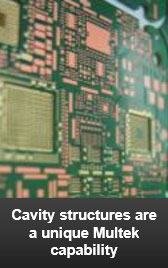
Today, Multek boasts the capabilities for up to 18+ layers of vertically-stacked and copper-filled µVias. Combined with additional innovations in 0.3mm fine-pitch package support, edge plating, and active cavity structures, Multek offers our customers the flexibility to meet any design challenges. These integrated processes are critical to the thin, high-density assemblies required in the smartphone, computing, IoT devices, modules, and many other products.
Multek is ready to provide you with end-to-end engineering and production services to bring your next-generation product PCB requirement seamlessly from NPI to mass production with world-class cycle times.