PCB Design & Layout

PCB Design & Layout
Got a new product idea?
Hetech’s engineering team will provide the highest-quality PCB design & layout services. We don’t just offer a one-size-fits-all solution. We carefully consider the purpose and requirements of a PCB before we begin the design process, ensuring it’s Designed for Manufacture, cost-effective & functional.
- Local Australian Support
- 30 Years’ of Developing Electronic Products
- Experienced In-house Engineering Team
- Cost-Effective Design
- Turnkey Development
- Design for Manufacturability
- Design for Environment
What is PCB design?
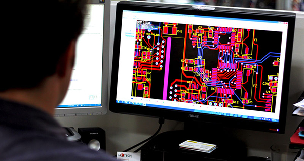
PCB design, or printed circuit board design, is the process where the layout of a PCB is created, to ensure when physically made, the PCB works efficiently. The design of a PCB has a significant impact on how it works and how reliable the product will be. The design process is usually started using software which innovatively merges component routing and placement before the circuit board is physically made.
Our design process
1. Specification
The first step the design process is to develop a clear specification of your product. Our design team will work with you to create your specification. This is the most important step as it will ensure that both parties have a clear scope and outcome for the project.
Subjects covered in the specification are (but not limited to):
- Desired functionalities and capabilities of the product
- The type of environment(s) that the product will be exposed to
- The life-cycle & expectancy
- Consideration of build materials
2. Proof of Concept
Using the Specifications, our engineers will then use off-the-shelf development kits to develop a “proof of concept”. This stage of the design will determine the types of technology used to achieve the goals of the product and whether the product concept is viable within the given budget and time-frame.
3. Schematic Capture & Design
The proof of concept will then be captured as schematic design. It shows all the components required and how they are connected. Think of the schematic design as a recipe, the ingredients are the components and all the engineers need to do is follow the recipe for the product build. Once the schematic for the circuit has been captured, simulations may take place to ensure the design is accurate.
4. PCB Component Placement and Routing
Using PCB design software such as Altium, all the required components on the working schematic design will be placed on a digital PCB board.
After our design team has placed all the components, connections between the components will be created, again following the schematic design “recipe”.
5. Design for Manufacture
Hetech will always ensure that your product is designed to conform to modern manufacturing practices. As an in-house Design and Manufacturing company, we have access to valuable direct manufacturing feedback. This will assist in reducing your manufacturing overheads.
6. Final Delivery
After extensive testing and revisions and all parties are happy, we have a final product!
Our team will export all your final design files and provide all documentation required to manufacture and operate your product. The PCB design will be as Gerber Files ready for the manufacturing process. A bill of materials will also be included to give information about specific components, materials and equipment required.